Timer A
Overview
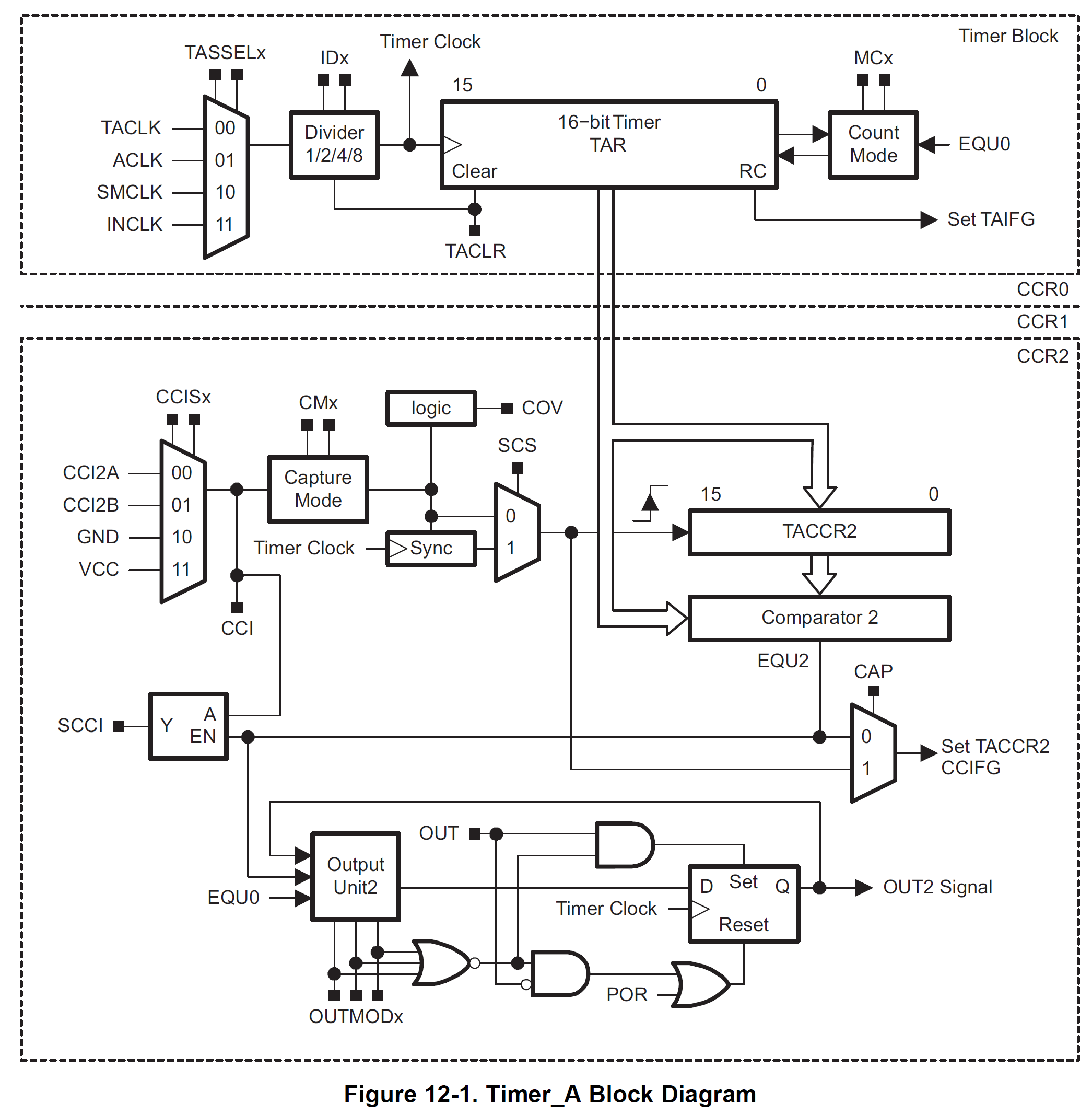
- Multiple input clock sources: mainly ACLK or SMCLK
- Additional clock divider
- 16-bit timer: Counts from 0 to 0xFFFF or 65535
- 3 so-called capture and compare register CCR0 to CCR2
- Capture mode:
- Copying timer's value to CCR on interrupt
- e.g. Measuring signal's frequency or periode
- Compare mode:
- Generating a interrupt, when timer's value is equal to CCR
- Automatically setting/toggling an output signal on equality
- Generating:
- symmetrical square waves (e.g. tone generator)
- PWM (pulse-with-modulated) signals (e.g. LED dimming, motor control, ...)
- Registers to control Timer A's functions:
Info
Timer A0 and A1 of MSP430G2553
The MSP430G2553 has two Timer A. In the following table the resulting register and interrupt names can be seen.
| Description | Timer A0 | Timer A1 |
|---|---|---|
| Timer A Control Register | TA0CTL | TA1CTL |
| Timer A Capture&Compare Register 0 | TA0CCR0 | TA1CCR0 |
| Timer A Capture&Compare Register 1 | TA0CCR1 | TA1CCR1 |
| Timer A Capture&Compare Register 2 | TA0CCR2 | TA1CCR2 |
| Timer A Capture&Compare Control Register 0 | TA0CCTL0 | TA1CCTL0 |
| Timer A Capture&Compare Control Register 1 | TA0CCTL1 | TA1CCTL1 |
| Timer A Capture&Compare Control Register 2 | TA0CCTL2 | TA1CCTL2 |
| Timer A Interrupt Vector 0 | TIMER0_A0_VECTOR | TIMER1_A0_VECTOR |
| Timer A Interrupt Vector 1 | TIMER0_A1_VECTOR | TIMER1_A1_VECTOR |
Generating Continuous Interrupt Signals
Using the CCR0
int main(void) {
WDTCTL = WDTPW | WDTHOLD; // stop watchdog timer
P1DIR |= BIT0;
TA0CCR0 = 0;
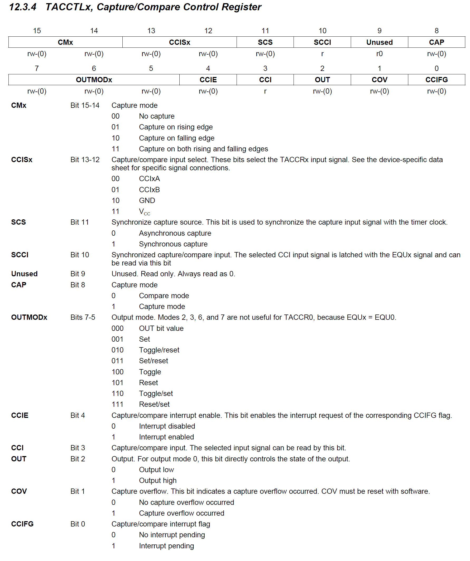
TA0CCTL0 = CCIE;
TA0CTL = TASSEL_1 + MC_2 + TACLR;
__enable_interrupt();
while (1) {
__low_power_mode_3();
}
}
#pragma vector=TIMER0_A0_VECTOR
__interrupt void TIMER0_A0_ISR() {
P1OUT ^= BIT0;
}
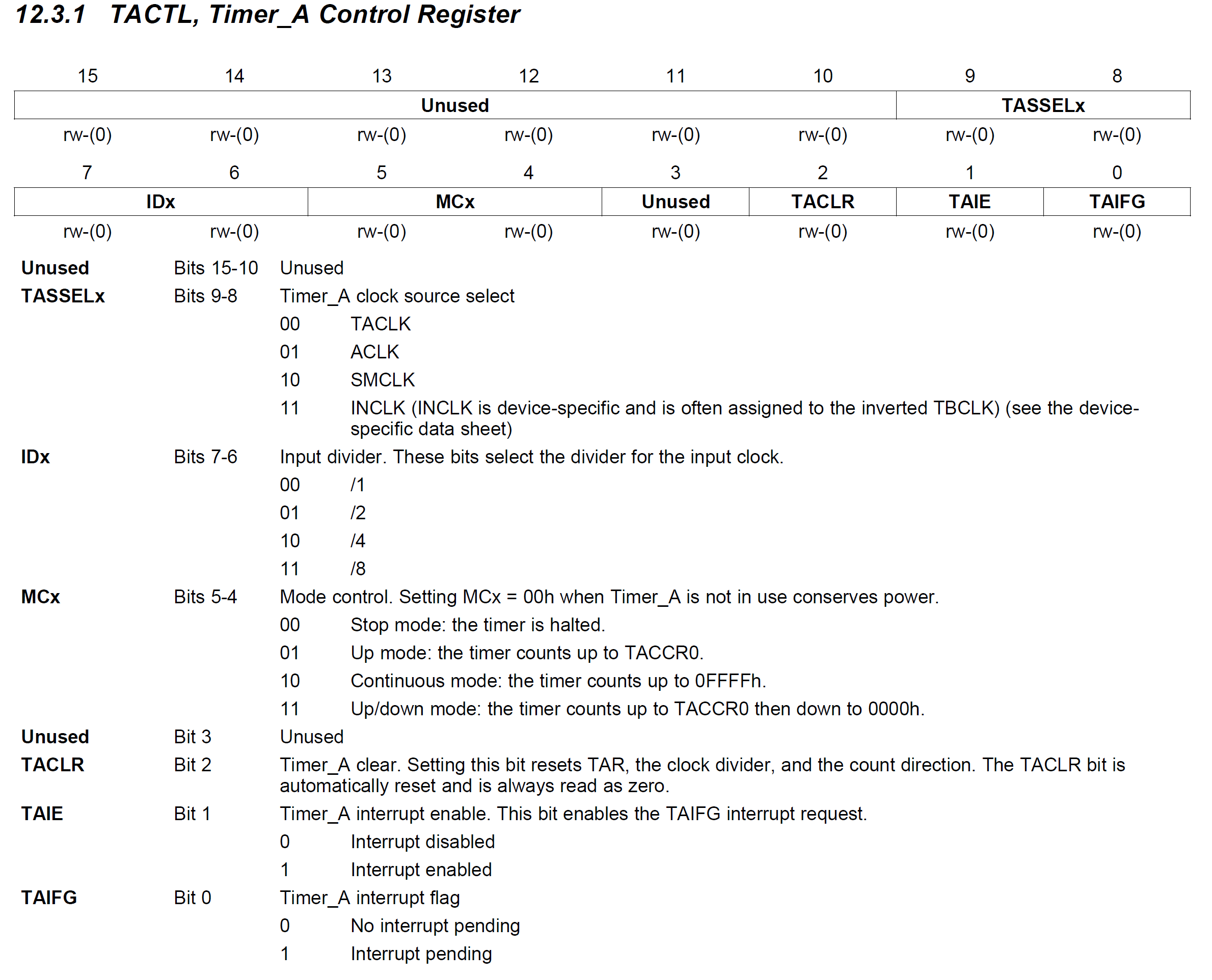
- Setting the bits in the registers TA0CCTL0 and TA0CTL as needed.
- Using the constants provided by the
msp430.hnamed after the datasheet.
Info
Multi-bit naming convention in msp430.h
Single-bit constants can be directly used as named in the datasheet.
e. g. TACLR is equal to BIT2 or 0x04
Multi-bit constants need to be distinguished between underscore and no-underscore convention. The following table is showing the difference in the mode control bits.
| Value | Description | Underscore Convention | No-Underscore Convention |
|---|---|---|---|
| 00 | Stop Mode | MC_0 |
0 |
| 01 | Up Mode | MC_1 |
MC0 |
| 10 | Continuous Mode | MC_2 |
MC1 |
| 11 | Up/Down Mode | MC_3 |
MC1 + MC0 |
Analysing the Program
TA0CCR0 = 0;- Setting the CCR to 0.
- Every time the timer counter will reach the value 0, a event will occur.
TA0CCTL0 = CCIE;- Compare mode →
CAP = 0 - Enabling the Interrupt →
CCIE = 0
- Compare mode →
TA0CTL = TASSEL_1 + MC_2 + TACLR;- use ACLK = 32.768 kHz →
TASSEL = 01 - no clock divider →
ID = 00 - starting timer in continuous mode →
MC = 10 - clearing the timer counter →
TACLR = 1
- use ACLK = 32.768 kHz →
__low_power_mode_3();- Enter LPM 3.
- ACLK needs to remain active, see Figure 3.2.
#pragma vector=TIMER0_A0_VECTOR
Interrupt Vector for the CCR0 interrupt

Info
Calculation of Timer Delays
Formular:
with \(\Delta t\) the time between two events, \(\Delta n\) the difference of the timer counter, or CCR value and \(f\) the input clock frequency of the timer.
With \(f = 32.768\si{kHz}\) the resulting delay times are:
| Δn (hex) | Δn (dec) | Δt [ms] |
|---|---|---|
| 0x4000 | 16384 | 500 |
| 0x8000 | 32768 | 1000 |
| 0xC000 | 49152 | 1500 |
| 0xFFFF | 65535 | 1999.97 |
| 0x10000 | 65536 | 2000 |
Blinking with 1 Hz
- In order to let the LED blink with an frequency of 1 Hz, the LED state needs to be changed (
P1OUT ^= BIT0;) once every 500 ms. - After the timer counted to 0x4000, an event needs to occur.
- Solution 1: Using the Up Mode of the Timer
- Up mode: the timer counts up to TACCR0
- setting TA0CCR0 to 0x4000 will generate an event every 500 ms.
TA0CCR0 = 0x4000;
TA0CCTL0 = CCIE;
TA0CTL = TASSEL_1 + MC_1 + TACLR;
- Solution 2: Using the Continuous Mode of the Timer
- Leaving the Timer in the Continuous Mode is a good practice in order to use CCR1 and CCR2 the same way. This can be seen in the following subsection.
- The ideas is to constantly change the CCR value in order to capture the next event at the correct time.
- In order to get correct interrupt at first the CCR0 needs to be 0x4000.
- To get an interrupt after 500 ms the next value needs to be 0x8000, then 0xC000, 0x0000 and 0x4000 again.
- This value change can be automatically calculated by executing
TA0CCR0 += 0x4000. - The overflow from 0xC000 + 0x4000 to 0x0000 is automatically done, because TA0CCR0 is a 16bit register.

TA0CCR0 = 0x4000;
TA0CCTL0 = CCIE;
TA0CTL = TASSEL_1 + MC_2 + TACLR;

...

#pragma vector=TIMER0_A0_VECTOR
__interrupt void TIMER0_A0_ISR() {
    P1OUT ^= BIT0;
    TA0CCR0 += 0x4000;
}
Using all CCR and the Timer Overflow Interrupt
- CCR1 and CCR2 can be used to generate interrupts, too.
- These interrupts are enabled by setting the CCIE flag in the corresponding TA0CCTLx register.
- Another interrupt source is the timer overflow. If the timer reaches the value 0xFFFF a interrupt is generated.
- This interrupt is enabled by setting the TAIE flag in the TA0CTL register.
- The following test program lets the RGB LEDs blink at different rates. Because the frequency is doubled from LED to LED all possible RGB colors will appear.
- The green LED (P1.0) will be toggled on timer overflow - once every two seconds.
int main(void) {
    ...

    P1OUT &= ~BIT0;
    P2OUT &= ~(BIT1 + BIT3 + BIT5);
    P1DIR |= BIT0;
    P2DIR |= BIT1 + BIT3 + BIT5;

    TA0CCR0 = 0x2000;
    TA0CCTL0 = CCIE;
    TA0CCR1 = 0x4000;
    TA0CCTL1 = CCIE;
    TA0CCR2 = 0x8000;
    TA0CCTL2 = CCIE;
    TA0CTL = TASSEL_1 + MC_2 + TACLR + TAIE;

    ...
}

#pragma vector=TIMER0_A0_VECTOR
__interrupt void TIMER0_A0_ISR() {
    P2OUT ^= BIT1;
    TA0CCR0 += 0x2000;
}

#pragma vector=TIMER0_A1_VECTOR
__interrupt void TimerA1_ISR() {
    switch (TAIV) {
    case 2:
        // CCR1 Interrupt
        P2OUT ^= BIT3;
        TA0CCR1 += 0x4000;
        break;
    case 4:
        // CCR2 Interrupt
        P2OUT ^= BIT5;
        TA0CCR2 += 0x8000;
        break;
    case 10:
        // Timer Overflow
        P1OUT ^= BIT0;
        break;
    }
}
- Because the timer can generate four different interrupts (3 by CCR + timer overflow) it can be expected that there are four different interrupt vectors and ISR.
- But the MSP430 only uses two ISR per timer to safe adress space.
- As you know from the port interrupts, ISR can be used by different interrupts sources. The interrupts flags needs to be read in order to identify the interrupts source.
- This is also true for the seconds ISR of the timer:
vector=TIMER0_A1_VECTOR - This ISR is used by the CCR1, CCR2 and timer overflow interrupt.
-
The following switch case structure should be used to identify the interrupt source:

Question
Modify the program using all CCRs to use only the Timer A1 instead of Timer A0. Change the corresponding register and interrupt vector names.