Parallel Interface - Inputs
Input Polling
- When using the inputs of the MSP430 the registers PxIN and PxREN are used.
- Detailed information of all MSP430 register can be found in the Family Guide.
- The correct Family Guide of the MSP430G2553 is called MSP430x2xx Family User's Guide and can be found under the address: https://www.ti.com/lit/ug/slau144j/slau144j.pdf
- The description of the registers PxIN and PxREN can be found on page 328
Info
Input Register PxIN
Each bit in each PxIN register reflects the value of the input signal at the corresponding I/O pin when the pin is configured as I/O function.
Bit = 0: The input is low
Bit = 1: The input is high
Output Registers PxOUT
Each bit in each PxOUT register is the value to be output on the corresponding I/O pin when the pin is configured as I/O function, output direction, and the pullup/down resistor is disabled.
Bit = 0: The output is low
Bit = 1: The output is high
If the pin's pullup/pulldown resistor is enabled, the corresponding bit in the PxOUT register selects pullup or pulldown.
Bit = 0: The pin is pulled down
Bit = 1: The pin is pulled up
Direction Registers PxDIR
Each bit in each PxDIR register selects the direction of the corresponding I/O pin, regardless of the selected function for the pin. PxDIR bits for I/O pins that are selected for other functions must be set as required by the other function.
Bit = 0: The port pin is switched to input direction
Bit = 1: The port pin is switched to output direction
Pullup/Pulldown Resistor Enable Registers PxREN
Each bit in each PxREN register enables or disables the pullup/pulldown resistor of the corresponding I/O pin. The corresponding bit in the PxOUT register selects if the pin is pulled up or pulled down.
Bit = 0: Pullup/pulldown resistor disabled
Bit = 1: Pullup/pulldown resistor enabled
Source: Family Guide, page 328f
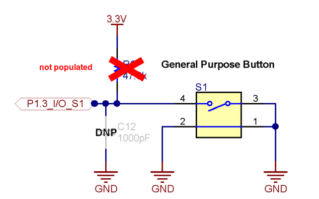
- When the button is pressed, P1.3 is connected to GND.
- To get always a valid logic level on P1.3 a pullup resistor is needed.
- The pullup resistor connects P1.3 to Vcc if the button is not pressed.
- If the button is pressed P1.3 is connected to GND. A small current flows through the pullup resistor.
Info
Button Pin Setup with pullup resistor
P1DIR &= ~BIT3;   // selecting input mode (default)
P1OUT |= BIT3;    // preparing OUT register to select pullup instead of pulldown
P1REN |= BIT3;    // enabling the pullup resistor
Using Pin State in a Condition
Waiting on Pin State
Question
Test the following two programs. Distinguish the working principle of the programs.
#include <msp430.h>
#include <stdint.h>

int main(void) {
    WDTCTL = WDTPW | WDTHOLD;  // stop watchdog timer

    P1DIR |= BIT0;

    P1DIR &= ~BIT3;
    P1OUT |= BIT3;
    P1REN |= BIT3;

    while (1) {
        if (!(P1IN & BIT3)) {
            P1OUT |= BIT0;
        } else {
            P1OUT &= ~ BIT0;
        }
    }
}
#include <msp430.h>
#include <stdint.h>

int main(void) {
    WDTCTL = WDTPW | WDTHOLD;  // stop watchdog timer

    P1DIR |= BIT0;

    P1DIR &= ~BIT3;
    P1OUT |= BIT3;
    P1REN |= BIT3;

    while (1) {
        while (!(P1IN & BIT3)) {
        }

        P1OUT ^= BIT0;

        while (P1IN & BIT3) {
        }
    }
}
Question
Modify your solution of previous task utilizing the RGB LED. Change the program to switch from one color to another by a button press.
Interrupts and Low Power Modes
Programming
Info
Polling vs. Interrupts
- What is difference between polling and interrupts?
- What we did in the last example with the
whileloop is called polling. The microcontroller continuously checks the state of the pin in order to monitor its level change. - When using a interrupt the level change is detected automatically. When this happens a special piece of code is executed - the so-called interrupt service routine (ISR).
- Real-world example: You are waiting a postal delivery:
- Polling: You are continuously walking downstairs to check whether the postman arrives.
- Interrupt: You are doing your studies. When the bell rings (Interrupt), you go downstairs to receive your delivery (ISR).
- Big advantage of Interrupts: The microcontroller can do something different while waiting on an interrupt (or save power by entering a low power mode [LPM]).
Info
Interrupt Flag Registers P1IFG, P2IFG
Each PxIFGx bit is the interrupt flag for its corresponding I/O pin and is set when the selected input signal edge occurs at the pin. All PxIFGx interrupt flags request an interrupt when their corresponding PxIE bit and the GIE bit are set. Each PxIFG flag must be reset with software. Software can also set each PxIFG flag, providing a way to generate a software initiated interrupt.
Bit = 0: No interrupt is pending
Bit = 1: An interrupt is pending
Only transitions, not static levels, cause interrupts. If any PxIFGx flag becomes set during a Px interrupt service routine, or is set after the RETI instruction of a Px interrupt service routine is executed, the set PxIFGx flag generates another interrupt. This ensures that each transition is acknowledged.
Interrupt Edge Select Registers P1IES, P2IES
Each PxIES bit selects the interrupt edge for the corresponding I/O pin.
Bit = 0: The PxIFGx flag is set with a low-to-high transition
Bit = 1: The PxIFGx flag is set with a high-to-low transition
Interrupt Enable P1IE, P2IE
Each PxIE bit enables the associated PxIFG interrupt flag.
Bit = 0: The interrupt is disabled.
Bit = 1: The interrupt is enabled.
Source: Family Guide, page 331f
int main(void) {
    WDTCTL = WDTPW | WDTHOLD;  // stop watchdog timer

    P1DIR |= BIT0;

    P1DIR &= ~BIT3;
    P1OUT |= BIT3;
    P1REN |= BIT3;
    P1IES |= BIT3;
    P1IFG &= ~BIT3;
    P1IE |= BIT3;

    __enable_interrupt();

    while (1) {
        __low_power_mode_4();
        P1OUT ^= BIT0;
    }
}

#pragma vector=PORT1_VECTOR
__interrupt void PORT1_ISR() {
    if (P1IFG & BIT3) {
        P1IFG &= ~BIT3;
        __low_power_mode_off_on_exit();
    }
}
__enable_interrupt();
Sets the Global Interrupt Enable (GIE).__low_power_mode_4();
Enters low power mode 4. Program stops on this point, until LPM is left again.#pragma vector=PORT1_VECTOR
__interrupt void PORT1_ISR()is the header of the ISR function
Compiler needs to add address of the function to interrupt vector.
MSP430 needs to known what function to execute on port interrupt.if (P1IFG & BIT3)
All interrupts on port 1 result intoPORT1_ISR()being executed. The IFG needs to be checked in order to find out interrupt sources.P1IFG &= ~BIT3;
Clearing the interrupt flag is mandatory.__low_power_mode_off_on_exit();
Leaving LPM. Program continues running atP1OUT ^= BIT0;.
Low Power Modes
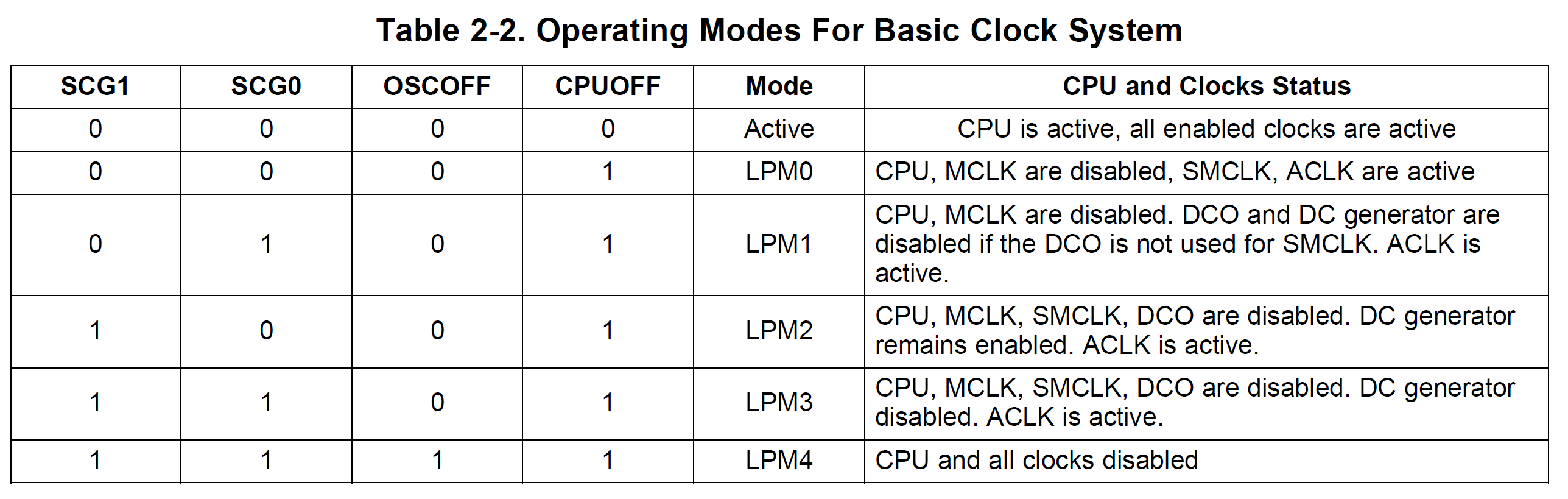
Basic Clock Module
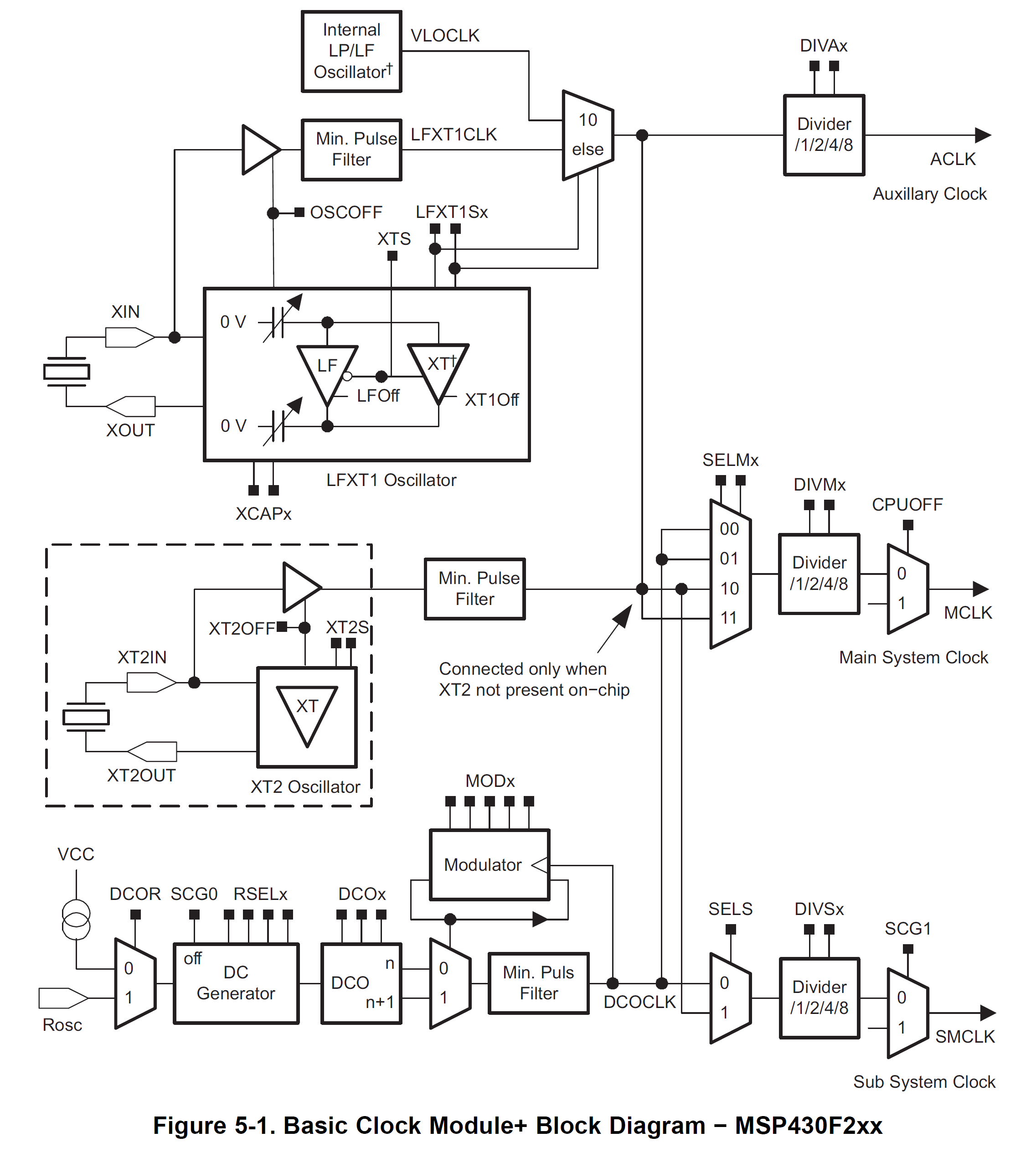
- Three different clock signals are generated by the BCM+:
- Auxillary Clock (ACLK)
- Main System Clock (MCLK)
- Sub System Clock (SMCLK)
- The system clocks are generated by the DCO (Digitally Controlled Oscillator).
- The default frequency of the DCO is around 1 MHz. The DCO can be calibrated to 1, 8, 12 or 16 MHz.
- The DCO output is used by MCLK and SMCLK. Additional dividers can be applied.
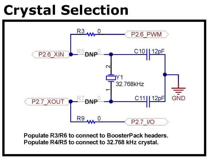
- The ACLK is fed by the low frequency oscillator (LFXT1).
- A clock crystal connected to pins P2.6 and P2.7 is used.
- The frequency of the ACLK is 32.768 kHz.
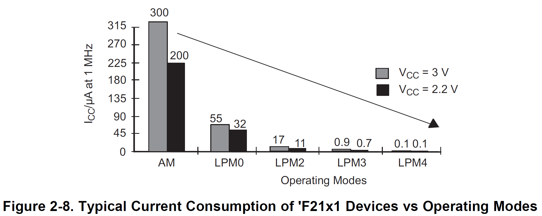
Current Measurement
Question
Measure the current consumption of the MSP430. Use a multimeter connected instead of the 3V3 Jumper on J101 (see Launchpad MSP-EXP430G2ET, page 11). Remove all other jumpers except GND to prevent current flowing into the programmer.
Solution
≈ 170 µA, LED turned off → + 1.1 mA
Question
The current consumption is highly influenced by floating pins. To remove the floating pins, enable the internal pulldown resistor on all unused pins.
P1OUT &= ~(BIT1 + BIT2 + BIT4 + BIT5 + BIT6 + BIT7);
P1REN |= BIT1 + BIT2 + BIT4 + BIT5 + BIT6 + BIT7;
P2OUT &= ~(BIT0 + BIT1 + BIT2 + BIT3 + BIT4 + BIT5);
P2REN |= BIT0 + BIT1 + BIT2 + BIT3 + BIT4 + BIT5;
Repeat your current measurement! Compare the value with the given in the datasheet (page 23).
Solution
≈ 124 nA, datasheet LPM4 25°C: 0.1–0.5 µA